| Style: | Hybrid PCB |
|---|---|
| Type: | Multilayer PCB |
| Pattern: | Horizontal |
| Material: | RO4350B and FR-4 |
| Brand Name: | Bicheng Enterprise Limited |
| Model Number: | BIC-0103-V103 |
| Place of Origin: | China (Mainland) |
| Surface Finishing: | Immersion Gold |
| Board Thickness: | 1.0mm |
| Copper Thickness: | 1.5 oz |
| Base Material: | RO4350B |
| Min. Line Spacing: | 5 mil |
| Min. Line Width: | 4.9 mil |
| Min. Hole Size: | 0.3mm |
| Solder Mask Color: | Green |
| Colour of Component Legend: | White |
| TEST: | 100% Electrical Test prior shipment |
Quick Details
Specifications
Brief Introduction
Just as its name implies, high frequency is that the frequency is relatively high, generally
Refers to the frequency of >=300 MHz (i.e. Wave length <=1m), that is, the usual radio
Frequency band. the electromagnetic wave of frequency >=1GHz is named microwave.
Typical frequencies for wireless applications:
* Current: 0.9GHz - 2GHz
* 3G systems: 2.5GHz
* Bluetooth: 2.5GHz
* GPS: 12.6GHz
* LMDS: 24GHz and 40GHz
* Automotive: 77GHz
Market: RFID, Wireless communications, base station and antenna, amplifier, military products,
Consumer electronics.
High frequency printed circuit board or microwave PCB refers to the printed circuit board made
on the high frequency (microwave) substrate copper clad plate. the common types are: Double
-sided board, multilayer board and mixed structure.
Mixed structure includes high performance special substrate, PP sheet + ordinary performance
Board and PP sheet mixed pressing board; high frequency substrate + ordinary FR4 substrate;
High frequency substrate + metal base etc.
PCB Case: 4 Layer High Frequency PCB Built on
RO4350B with Blind Via and Immersion Gold
(PCB's are custom-made products, the picture and parameters shown are just for
Reference)
General Description
this is a type of 4-layer HDI high frequency PCB circuit board built on RO4350B with
RO4450B prepreg for the application of radar RF board. It's a multilayer layer RF PCB
Board at 1.0 mm thick with immersion gold finish and solder mask and silkscreen. this
Board contains blind via from top layer to inner 1, top layer to inner 3. since it's asymmetric
Buildup, 1.2% warpage is allowed. It's fabricated per IPC 6012 Class 2 using supplied Gerber
Data. Each 20 boards are packed for shipment.
Features and benefits
the temperature coefficient of dielectric constant is among the lowest of any circuit
Board material, making it ideal for temperature sensitive applications.
Reducing signal loss in high frequency application meets the development needs of
Communication technology.
Excellent high frequency performance due to low dielectric tolerance and loss.
Gold has high solderability, no stressing of circuit boards and less contamination of
PCB surface.
Engineering design prevents problems from occurring in pre-production.
100% tests inclusive of electrical test and AOI inspection.
Fast and flexible to save the time of production from prototype to standard production
Great customer service
UL recognized and RoHS Directive-compliant
Application
RF module, Power splitter, Low Noise Block, 3G antenna
Parameter and data sheet
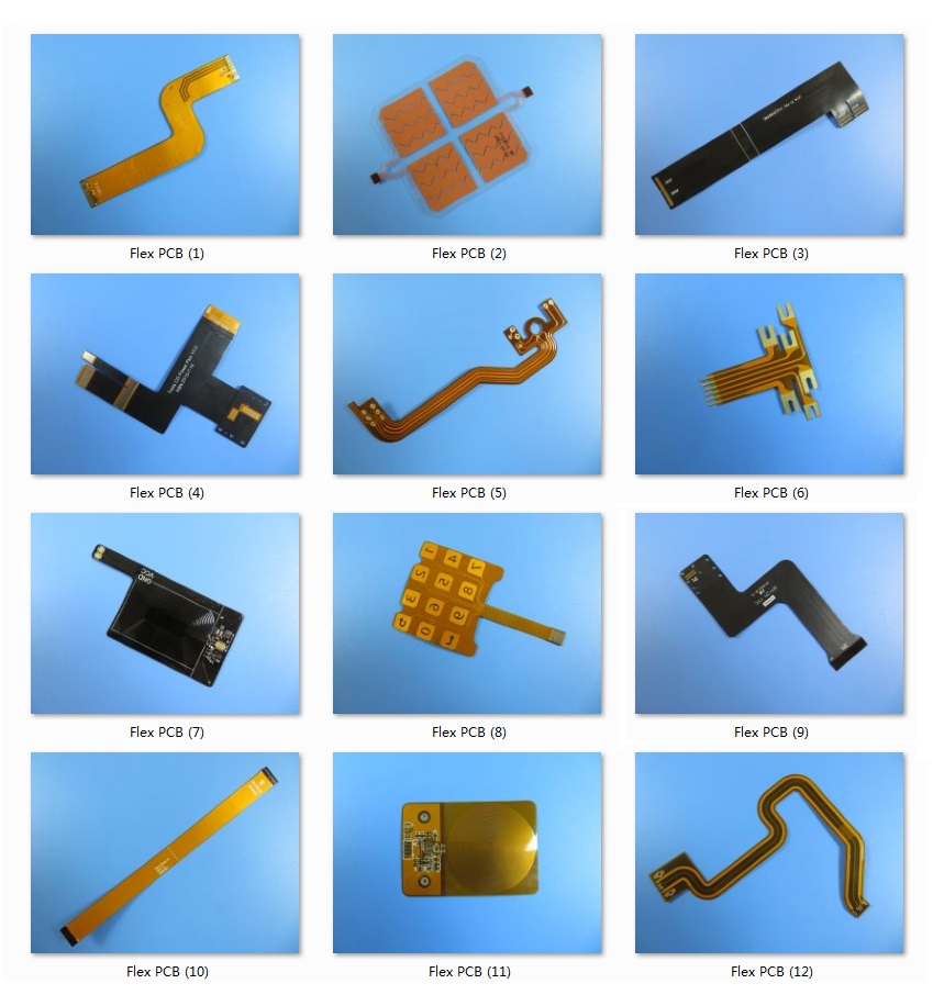
Variety of PCBs

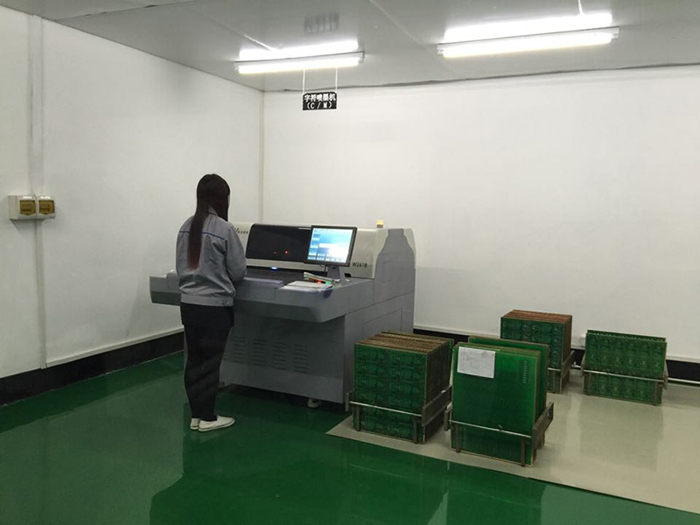
Legend inkjet printer

Just as its name implies, high frequency is that the frequency is relatively high, generally
Refers to the frequency of >=300 MHz (i.e. Wave length <=1m), that is, the usual radio
Frequency band. the electromagnetic wave of frequency >=1GHz is named microwave.
Typical frequencies for wireless applications:
* Current: 0.9GHz - 2GHz
* 3G systems: 2.5GHz
* Bluetooth: 2.5GHz
* GPS: 12.6GHz
* LMDS: 24GHz and 40GHz
* Automotive: 77GHz
Market: RFID, Wireless communications, base station and antenna, amplifier, military products,
Consumer electronics.
High frequency printed circuit board or microwave PCB refers to the printed circuit board made
on the high frequency (microwave) substrate copper clad plate. the common types are: Double
-sided board, multilayer board and mixed structure.
Mixed structure includes high performance special substrate, PP sheet + ordinary performance
Board and PP sheet mixed pressing board; high frequency substrate + ordinary FR4 substrate;
High frequency substrate + metal base etc.
PCB Case: 4 Layer High Frequency PCB Built on
RO4350B with Blind Via and Immersion Gold
(PCB's are custom-made products, the picture and parameters shown are just for
Reference)
General Description
this is a type of 4-layer HDI high frequency PCB circuit board built on RO4350B with
RO4450B prepreg for the application of radar RF board. It's a multilayer layer RF PCB
Board at 1.0 mm thick with immersion gold finish and solder mask and silkscreen. this
Board contains blind via from top layer to inner 1, top layer to inner 3. since it's asymmetric
Buildup, 1.2% warpage is allowed. It's fabricated per IPC 6012 Class 2 using supplied Gerber
Data. Each 20 boards are packed for shipment.
Features and benefits
the temperature coefficient of dielectric constant is among the lowest of any circuit
Board material, making it ideal for temperature sensitive applications.
Reducing signal loss in high frequency application meets the development needs of
Communication technology.
Excellent high frequency performance due to low dielectric tolerance and loss.
Gold has high solderability, no stressing of circuit boards and less contamination of
PCB surface.
Engineering design prevents problems from occurring in pre-production.
100% tests inclusive of electrical test and AOI inspection.
Fast and flexible to save the time of production from prototype to standard production
Great customer service
UL recognized and RoHS Directive-compliant
Application
RF module, Power splitter, Low Noise Block, 3G antenna
Parameter and data sheet
| PCB SIZE | 98.02 x 101.02 mm =1up |
| BOARD TYPE | HDI PCB, High frequency PCB |
| Number of Layers | 4 layers |
| Surface Mount Components | YES |
| through Hole Components | YES |
| LAYER STACKUP | Copper ------- 35um(1 oz)+plate TOP layer |
| RO4350B 6.6mil | |
| Inner Layer 1, 18um (0.5oz) | |
| Dielectric RO4450B 4mil x2 | |
| Inner Layer 2, 18um (0.5oz) | |
| Dielectric RO4350B 20mil | |
| Copper ------- 35um(1oz) + plate BOT Layer | |
| TECHNOLOGY | |
| Minimum Trace and Space: | 5 mil / 4.9 mil |
| Minimum / Maximum Holes: | 0.3 mm / 5.5 mm |
| Number of Different Holes: | 10 |
| Number of Drill Holes: | 125 |
| Number of Milled Slots: | 0 |
| Number of Internal Cutouts: | 0 |
| Impedance Control: | no |
| Number of Gold finger: | 0 |
| BOARD MATERIAL | |
| Glass Epoxy: | RO4350B Tg280, er<3.48, Rogers Corp. |
| Final foil external: | 1.5 oz |
| Final foil internal: | 0.5 oz |
| Final height of PCB: | 1.0 mm 10% |
| PLATING and COATING | |
| Surface Finish | Immersion gold, 35% |
| Solder Mask Apply to: | TOP, 12micron Minimum |
| Solder Mask Color: | Green, PSR-2000GT600D, Taiyo Supplied. |
| Solder Mask Type: | LPSM |
| CONTOUR/CUTTING | CNC Routing |
| MARKING | |
| Side of Component Legend | TOP |
| Colour of Component Legend | White, IJR-4000 MW300, Taiyo brand |
| Manufacturer Name or Logo: | Marked on the board in a conductor and leged FREE AREA |
| VIA | Plated through hole(PTH), minimum size 0.3mm. Blind via L1-L2, L1-L3 |
| FLAMIBILITY RATING | UL 94-V0 Approval MIN. |
| DIMENSION TOLERANCE | |
| Outline dimension: | 0.0059" |
| Board plating: | 0.0029" |
| Drill tolerance: | 0.002" |
| TEST | 100% Electrical Test prior shipment |
| TYPE of ARTWORK to BE SUPPLIED | Gerber RS-274-X, PCBDOC etc |
| SERVICE AREA | Worldwide, Globally. |
Variety of PCBs
Legend inkjet printer


