| Surface Finishing: | Hot Air Soldering Leveling(HASL),lead free |
|---|---|
| Board Thickness: | 1.6mm |
| Copper Thickness: | 1 oz |
| Base Material: | 1W/MK dielectric material, MCPCB |
| Brand Name: | Bicheng Enterprise Limited |
| Min. Line Spacing: | 10 mil |
| Min. Line Width: | 12 mil |
| Min. Hole Diameter: | 1.5mm |
| Model Number: | BIC-776-V776 |
| Place of Origin: | China (Mainland) |
| Solder Mask Color: | White |
| Color of Silkscreen: | Black |
| TEST: | 100% Electrical Test prior shipment |
Quick Details
Specifications
Mirror Aluminum PCB
the mirror aluminum PCB is a substrate which is pressed together with BT material circuit
Layer and aluminum substrate with silver particles. It is the most suitable raw material for
COB packaging.
Advantages
Good heat dissipation: the mirror silver aluminum substrate adopts thermoelectric separation
Technology, and the thermal conductivity of ordinary aluminum PCB with insulating layer is
1W/MK to 3W/MK. the thermal conductivity of mirror aluminum PCB reaches higher 137W/MK,
Which greatly improves the heat dissipation of the chip.
High light efficiency: the reflectivity of the ordinary gold aluminum PCB is 80%, the reflectivity
of the cup hole aluminum PCB is 85%, the reflectivity of the silver plated aluminum PCB is 95%,
and the reflectivity of the mirror silver aluminum PCB is 98%. the mirror silver aluminum PCB
Can make the light of the chip better excited.
PCB Services
1) Prototype, small runs and mass production supply
2) V-Groove, Punch, CNC mill
3) ENIG, HASL, OSP and Immersion tin
4) No MOQ
5) Door to door shipping service

Aluminum PCB Case: Mirror Aluminum Base PCB in
Panel for Chip on Board Package
(PCB's are custom-made products, the picture and parameters shown are just for reference)
General description
this is a type of Single layer Aluminum 2.0mm board for the application of LED lighting with
HASL pad finish. the base laminate is from ITEQ, White Solder mask from Taiyo and Black
Silkscreen from Taiyo too. It's fabricated per IPC 6012 Class 2 using supplied Gerber data.
Each 20 panel boards are packed separately.
Features and benefits
Optimization combination of power circuit and control circuit,
Replace the fragile ceramic substrate and obtain a better mechanical durability,
Effective heat diffusion in the design of the circuit,
Reduce the operating temperature of the equipment,
Improve the power density and reliability of the device,
Prolong the service life of the product,
100% tests inclusive of electrical test and AOI inspection.
UL, ISO certified PCB manufacturing factory.
Make delivery on time keeping 98% on-time-delivery rate.
International approvals
UL recognized and RoHS Directive-compliant
RoHS materials
Application
Projector lamp, Automatic safety control system, Switch regulator, preamplifier
MCPCB Capability
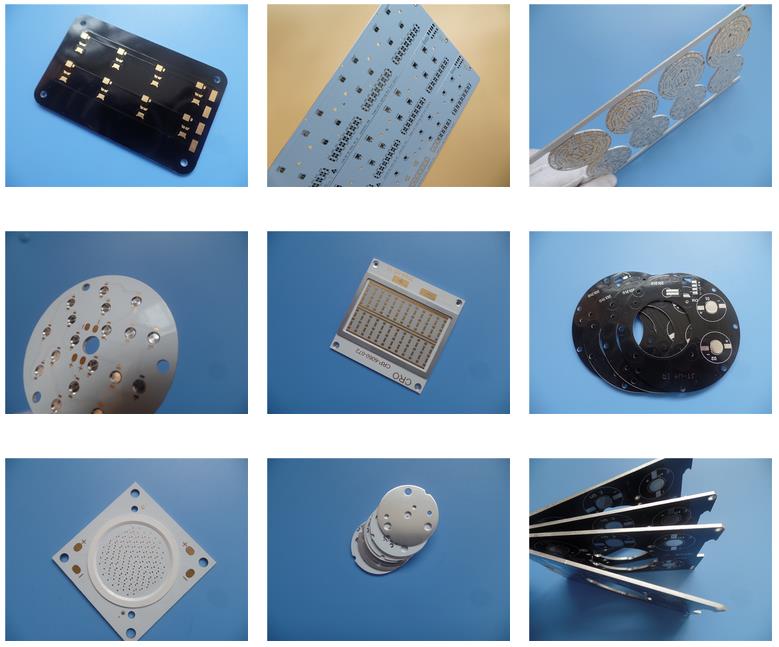
Variety of PCBs


the mirror aluminum PCB is a substrate which is pressed together with BT material circuit
Layer and aluminum substrate with silver particles. It is the most suitable raw material for
COB packaging.
Advantages
Good heat dissipation: the mirror silver aluminum substrate adopts thermoelectric separation
Technology, and the thermal conductivity of ordinary aluminum PCB with insulating layer is
1W/MK to 3W/MK. the thermal conductivity of mirror aluminum PCB reaches higher 137W/MK,
Which greatly improves the heat dissipation of the chip.
High light efficiency: the reflectivity of the ordinary gold aluminum PCB is 80%, the reflectivity
of the cup hole aluminum PCB is 85%, the reflectivity of the silver plated aluminum PCB is 95%,
and the reflectivity of the mirror silver aluminum PCB is 98%. the mirror silver aluminum PCB
Can make the light of the chip better excited.
PCB Services
1) Prototype, small runs and mass production supply
2) V-Groove, Punch, CNC mill
3) ENIG, HASL, OSP and Immersion tin
4) No MOQ
5) Door to door shipping service
Aluminum PCB Case: Mirror Aluminum Base PCB in
Panel for Chip on Board Package
(PCB's are custom-made products, the picture and parameters shown are just for reference)
General description
this is a type of Single layer Aluminum 2.0mm board for the application of LED lighting with
HASL pad finish. the base laminate is from ITEQ, White Solder mask from Taiyo and Black
Silkscreen from Taiyo too. It's fabricated per IPC 6012 Class 2 using supplied Gerber data.
Each 20 panel boards are packed separately.
Features and benefits
Optimization combination of power circuit and control circuit,
Replace the fragile ceramic substrate and obtain a better mechanical durability,
Effective heat diffusion in the design of the circuit,
Reduce the operating temperature of the equipment,
Improve the power density and reliability of the device,
Prolong the service life of the product,
100% tests inclusive of electrical test and AOI inspection.
UL, ISO certified PCB manufacturing factory.
Make delivery on time keeping 98% on-time-delivery rate.
International approvals
UL recognized and RoHS Directive-compliant
RoHS materials
Application
Projector lamp, Automatic safety control system, Switch regulator, preamplifier
MCPCB Capability
| NO. | Parameter | Value |
| 1 | Type of Metal Core | Aluminum, Copper, Iron |
| 2 | Model of Metal Core | A1100, A5052, A6061, A6063, C1100 |
| 3 | Surface Finish | HASL, Immersion Gold, Immersion Silver, OSP |
| 4 | Thickness of Surface plating | HASL: Sn>2.54M, ENIG: Au 0.025-0.1m, Ni 2.5-5m |
| 5 | Layer Count | 1-4 Layers |
| 6 | Maximum of Board Size | 23" x 46" (584mm1168mm) |
| 7 | Mininum of Board Size | 0.1969" x 0.1969" (5mm5mm) |
| 8 | Board Thickness | 0.0157" x 0.2362" (0.4-6.0mm) |
| 9 | Copper Thickness | 0.5OZ(17.5m),1OZ(35m),2OZ(70m), 3OZ(105m),4OZ(140m) to 10oz (350m) |
| 10 | Minimum Track Width | 5mil (0.127mm) |
| 11 | Minimum Space | 5mil (0.127mm) |
| 12 | Minimum Hole Size | 0.0197" (0.5mm) |
| 13 | Maximum Hole Size | No limit |
| 14 | Minimum Holes Punched | PCB thickness <1.0mm: 0.0394" (1.0mm) |
| PCB thikness 1.2-3.0mm: 0.0591" (1.5mm) | ||
| 15 | PTH Wall Thickness | >20m |
| 16 | Tolerance of PTH | 0.00295" (0.075mm) |
| 17 | Tolerance of NPTH | 0.00197" (0.05mm) |
| 18 | Deviation of Hole Position | 0.00394" (0.10mm) |
| 19 | Outline Tolerance | Routing: 0.00394" (0.1mm) |
| Punching: 0.00591" (0.15mm) | ||
| 20 | Angle of V-cut | 30, 45, 60 |
| 21 | V-cut Size | 0.1969" x 47.24" (5mm1200mm) |
| 22 | Thickness of V-cut Board | 0.0236" x 0.1181" (0.6-3mm) |
| 23 | Tolerance of V-cut Angle | 5 |
| 24 | V-CUT Verticality | 0.0059" (0.15mm) |
| 25 | Minimum Square Slots Punched | PCB thickness < 1.0mm: 0.0315" x 0.0315" (0.8 x 0.8mm) |
| PCB thickness 1.2-3.0mm: 0.0394" x 0.0394" (1.0 x 1.0mm) | ||
| 26 | Minimum BGA PAD | 0.01378" (0.35mm) |
| 27 | Minimum Width of Solder Mask Bridge. | 8mil (0.2032mm) |
| 28 | Minimum Thickness of Solder Mask | >13M (0.013mm) |
| 29 | Insulation Resistance | 1012Normal |
| 30 | Peel-off Strength | 2.2N/mm |
| 31 | Solder float | 260 3min |
| 32 | E-test Voltage | 50-250V |
| 33 | Thermal Conductivity | 0.8-8W/M.K |
| 34 | Warp or Twist | 0.5% |
| 35 | Flammability | FV-0 |
| 36 | Minimum Height of Component indicator | 0.0059"(0.15mm) |
| 37 | Minimum Open Solder Mask on Pad | 0.000394" (0.01mm) |
Variety of PCBs


