| Surface Finishing: | OSP |
|---|---|
| Board Thickness: | 1.2mm |
| Copper Thickness: | 10 OZ |
| Base Material: | 1W/MK dielectric material, MCPCB |
| Brand Name: | Bicheng Enterprise Limited |
| Min. Line Spacing: | 70 mil |
| Min. Line Width: | 70 mil |
| Min. Hole Diameter: | N/A |
| Model Number: | BIC-784-V784 |
| Place of Origin: | China (Mainland) |
| Solder Mask Color: | N/A |
| Colour of Component Legend: | N/A |
| TEST: | 100% Electrical Test prior shipment |
Quick Details
Specifications
Structure of MCPCB
the most common MCPCB construction consists of the following layers:
1) A metal substrate, typically aluminum. In some applications, a copper substrate is more
Appropriate due to its high thermal conductivity than aluminum (401W/MK versus 237 W/MK)
but more expensive.
2) Epoxy dielectric layer. this is the most important layer in the MCPCB construction as it
Affects the thermal performance, electrical breakdown strength, and, in some cases, the
Solder joint performance of the MCPCB system. the typical thermal conductivity of the
Dielectric layer on a MCPCB is 1W/MK. A higher value is better for good thermal performance.
A thinner dielectric layer is better for thermal performance as well but can negatively impact
the ability of the MCPCB to withstand a high potential test to meet minimum electrical safety
Standards as required in certain lighting markets. the typical dielectric thickness layer is 100m.
3) Top copper layer. A thicker copper layer improves heat spreading into the PCB but may
Pose challenges for PCB manufacturers when fabricating narrow traces or spaces. A copper
Thickness of 1oz (35m) or 2oz (70m) is common.

Aluminum PCB Case: Heavy Copper PCB Built on
Aluminum Base with 10 Oz Copper Weight
(PCB's are custom-made products, the picture and parameters shown are just for reference)
General description
this is a type of heavy copper PCB built on aluminum substrate with breakdown voltage
4000 VDC for the application of Large-current application. It's 1.2 mm thick without
Silkscreen and solder mask and a coating of OSP on pads. the base material is from
Totking supplying single up PCB. They're fabricated per IPC 6012 Class 2 using supplied
Gerber data. Each 25 panels are packed for shipment.
Features and benefits
Optimization combination of power circuit and control circuit
Better heat dissipation of high heat generated by large current
PCB manufacturing is on required specifications.
8000 types of PCB per month
Quick Lead time: 3-5 days
Free-of-charge PCB panelization
Application
Uninterrupted Power Supply, Desktop Power Supply, Computer Power Supplies, Battery
Power Supply, Inverter Power,Power Supply Components, DVE Power Supply,Electric
Vehicle charging (commercial and industrial), AC AC Converter, 2000W Inverter
Parameter and data sheet
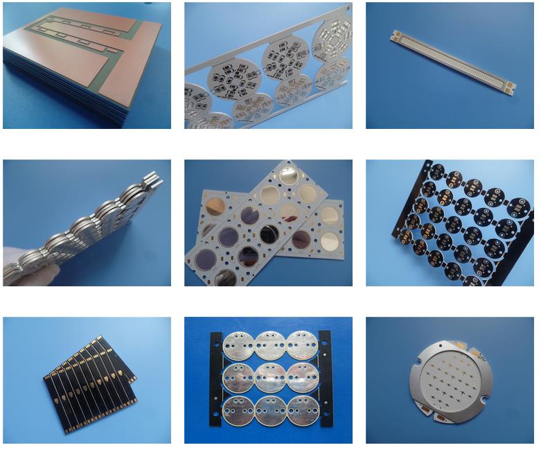
Variety of PCBs

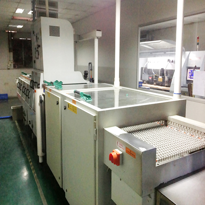
PCB board washing

the most common MCPCB construction consists of the following layers:
1) A metal substrate, typically aluminum. In some applications, a copper substrate is more
Appropriate due to its high thermal conductivity than aluminum (401W/MK versus 237 W/MK)
but more expensive.
2) Epoxy dielectric layer. this is the most important layer in the MCPCB construction as it
Affects the thermal performance, electrical breakdown strength, and, in some cases, the
Solder joint performance of the MCPCB system. the typical thermal conductivity of the
Dielectric layer on a MCPCB is 1W/MK. A higher value is better for good thermal performance.
A thinner dielectric layer is better for thermal performance as well but can negatively impact
the ability of the MCPCB to withstand a high potential test to meet minimum electrical safety
Standards as required in certain lighting markets. the typical dielectric thickness layer is 100m.
3) Top copper layer. A thicker copper layer improves heat spreading into the PCB but may
Pose challenges for PCB manufacturers when fabricating narrow traces or spaces. A copper
Thickness of 1oz (35m) or 2oz (70m) is common.
Aluminum PCB Case: Heavy Copper PCB Built on
Aluminum Base with 10 Oz Copper Weight
(PCB's are custom-made products, the picture and parameters shown are just for reference)
General description
this is a type of heavy copper PCB built on aluminum substrate with breakdown voltage
4000 VDC for the application of Large-current application. It's 1.2 mm thick without
Silkscreen and solder mask and a coating of OSP on pads. the base material is from
Totking supplying single up PCB. They're fabricated per IPC 6012 Class 2 using supplied
Gerber data. Each 25 panels are packed for shipment.
Features and benefits
Optimization combination of power circuit and control circuit
Better heat dissipation of high heat generated by large current
PCB manufacturing is on required specifications.
8000 types of PCB per month
Quick Lead time: 3-5 days
Free-of-charge PCB panelization
Application
Uninterrupted Power Supply, Desktop Power Supply, Computer Power Supplies, Battery
Power Supply, Inverter Power,Power Supply Components, DVE Power Supply,Electric
Vehicle charging (commercial and industrial), AC AC Converter, 2000W Inverter
Parameter and data sheet
| PCB SIZE | 75 x 64mm=1PCS |
| BOARD TYPE | Aluminum PCB, IMS PCB |
| Number of Layers | Single sided PCB |
| Surface Mount Components | YES |
| through Hole Components | NO |
| LAYER STACKUP | Copper ------- 350 um(10 oz) |
| 1W/MK dielectric material | |
| Aluminum 5052 0.8mm | |
| TECHNOLOGY | |
| Minimum Trace and Space: | 70 mil / 70 mil |
| Minimum / Maximum Holes: | N/A |
| Number of Different Holes: | N/A |
| Number of Drill Holes: | N/A |
| Thermal resistance(C/W) | 0.45 |
| Breakdown Voltage(VDC) | 4000 |
| Impedance Control | no |
| BOARD MATERIAL | |
| Thermal conductivity | 1W/MK dielectric material, MCPCB |
| Final foil external: | 10 OZ |
| Final foil internal: | 0 oz |
| Final height of PCB: | 1.2mm 0.12 |
| PLATING and COATING | |
| Surface Finish | OSP |
| Solder Mask Apply to: | N/A |
| Solder Mask Color: | N/A |
| Solder Mask Type: | N/A |
| CONTOUR/CUTTING | Routing |
| MARKING | |
| Side of Component Legend | N/A |
| Colour of Component Legend | N/A |
| Manufacturer Name or Logo: | N/A |
| VIA | No via |
| FLAMIBILITY RATING | UL 94-V0 Approval MIN. |
| DIMENSION TOLERANCE | |
| Outline dimension: | 0.0059" (0.15mm) |
| Board plating: | 0.0030" (0.076mm) |
| Drill tolerance: | 0.002" (0.05mm) |
| TEST | 100% Electrical Test prior shipment |
| TYPE of ARTWORK to BE SUPPLIED | Gerber RS-274-X, PCBDOC etc |
| SERVICE AREA | Worldwide, Globally. |
Variety of PCBs
PCB board washing


