| Surface Finishing: | Immersion gold |
|---|---|
| Board Thickness: | 1.0mm |
| Copper Thickness: | 1.0 OZ |
| Base Material: | 1W/MK dielectric material 75um |
| Brand Name: | Bicheng Enterprise Limited |
| Min. Line Spacing: | N/A |
| Min. Line Width: | N/A |
| Min. Hole Diameter: | N/A |
| Model Number: | BIC-814-V814 |
| Place of Origin: | China (Mainland) |
| Solder mask Colour: | Black |
| Silkscreen Color: | White |
| TEST: | 100% Electrical Test prior shipment |
Quick Details
Specifications
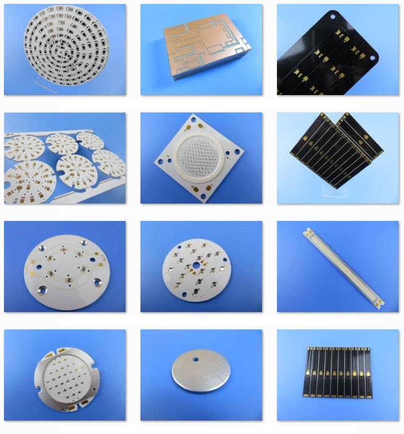
Copper Core PCB with Convex Plate for Solar Energy
Collection
(PCB's are custom-made products, the picture and parameters shown are just for reference)
Copper core PCB is one of the most expensive metal substrates, and its thermal conductivity
Is many times better than that of aluminum and iron substrates. It is suitable for high frequency
Circuits, high and low temperature changing regions and the heat dissipation and building
Decoration industries of precision communication equipment.
the circuit layer of copper substrate is required to have a large current-carrying capacity,
so a thick copper foil should be used, the thickness of which is generally 35 m ~ 280 m;
Thermal insulation layer is the core technology of copper substrate too. The core thermal
Conductivity is composed of aluminum trioxide and silicon powder and polymer filled with
Epoxy resin, the thermal resistance is low (0.15), viscoelasticity is excellent, and it has the
Ability to resist thermal aging. It is able to withstand mechanical and thermal stress.
Metal base is the support member of copper PCB. It is required to have high thermal
Conductivity, generally copper sheet is used because copper can provide better thermal
Conductivity, suitable for drilling, punching, shearing and cutting and other conventional
Machining.

Metal Core PCB Capability 2019
Copper Core PCB
1) Single sided, double sided.
2) Insulated metal substrate (IMS PCB) and Metal core PCB (MCPCB)
3) V-Groove, Punch, CNC milling
4) ENIG, HASL, OSP and Immersion tin
5) Solder mask: Black, White and Green
MCPCB

MCPCB

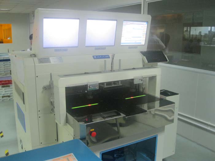
Inner Etching Alignment and hole-shooting Machine


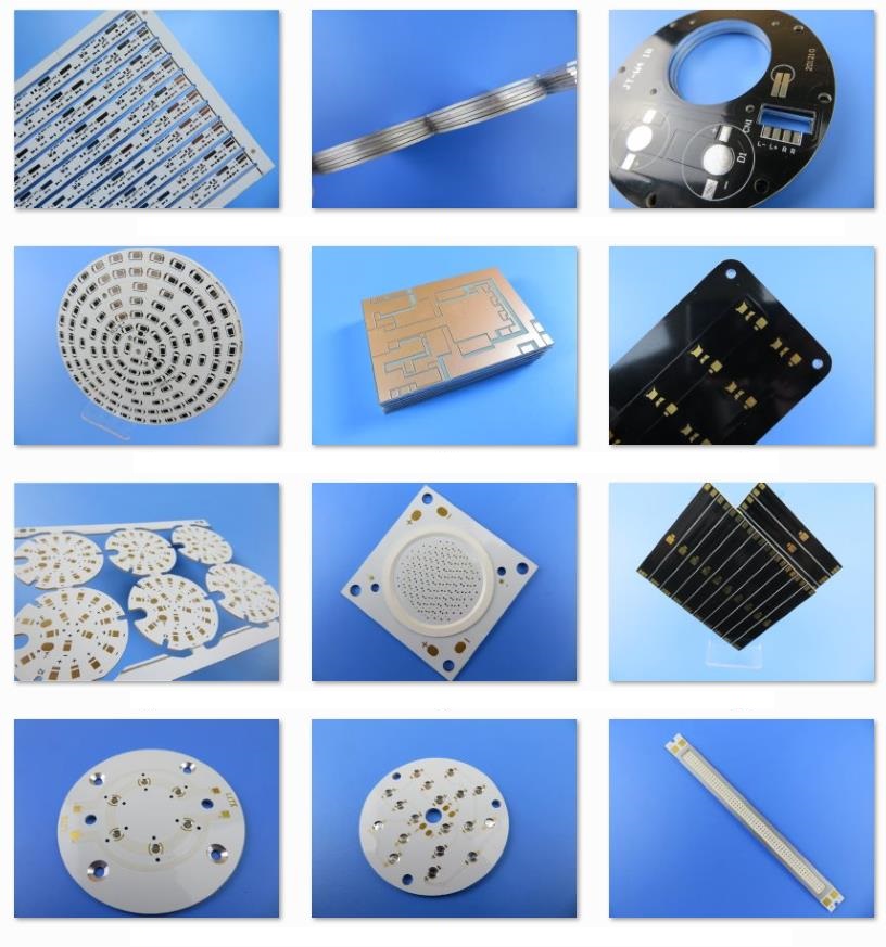
Collection
(PCB's are custom-made products, the picture and parameters shown are just for reference)
Copper core PCB is one of the most expensive metal substrates, and its thermal conductivity
Is many times better than that of aluminum and iron substrates. It is suitable for high frequency
Circuits, high and low temperature changing regions and the heat dissipation and building
Decoration industries of precision communication equipment.
the circuit layer of copper substrate is required to have a large current-carrying capacity,
so a thick copper foil should be used, the thickness of which is generally 35 m ~ 280 m;
Thermal insulation layer is the core technology of copper substrate too. The core thermal
Conductivity is composed of aluminum trioxide and silicon powder and polymer filled with
Epoxy resin, the thermal resistance is low (0.15), viscoelasticity is excellent, and it has the
Ability to resist thermal aging. It is able to withstand mechanical and thermal stress.
Metal base is the support member of copper PCB. It is required to have high thermal
Conductivity, generally copper sheet is used because copper can provide better thermal
Conductivity, suitable for drilling, punching, shearing and cutting and other conventional
Machining.
Metal Core PCB Capability 2019
| NO. | Parameter | Value |
| 1 | Type of Metal Core | Aluminum, Copper, Iron |
| 2 | Model of Metal Core | A1100, A5052, A6061, A6063, C1100 |
| 3 | Surface Finish | HASL, Immersion Gold, Immersion Silver, OSP |
| 4 | Thickness of Surface plating | HASL: Sn>2.54M, ENIG: Au 0.025-0.1m, Ni 2.5-5m |
| 5 | Layer Count | 1-4 Layers |
| 6 | Maximum of Board Size | 23" x 46" (584mm1168mm) |
| 7 | Mininum of Board Size | 0.1969" x 0.1969" (5mm5mm) |
| 8 | Board Thickness | 0.0157" x 0.2362" (0.4-6.0mm) |
| 9 | Copper Thickness | 0.5OZ(17.5m),1OZ(35m),2OZ(70m) 3OZ(105m),4OZ(140m) to 10oz (350m) |
| 10 | Minimum Track Width | 5mil (0.127mm) |
| 11 | Minimum Space | 5mil (0.127mm) |
| 12 | Minimum Hole Size | 0.0197" (0.5mm) |
| 13 | Maximum Hole Size | No limit |
| 14 | Minimum Holes Punched | PCB thickness <1.0mm: 0.0394" (1.0mm) |
| PCB thikness 1.2-3.0mm: 0.0591" (1.5mm) | ||
| 15 | PTH Wall Thickness | >20m |
| 16 | Tolerance of PTH | 0.00295" (0.075mm) |
| 17 | Tolerance of NPTH | 0.00197" (0.05mm) |
| 18 | Deviation of Hole Position | 0.00394" (0.10mm) |
| 19 | Outline Tolerance | Routing: 0.00394" (0.1mm) |
| Punching: 0.00591" (0.15mm) | ||
| 20 | Angle of V-cut | 30, 45, 60 |
| 21 | V-cut Size | 0.1969" x 47.24" (5mm1200mm) |
| 22 | Thickness of V-cut Board | 0.0236" x 0.1181" (0.6-3mm) |
| 23 | Tolerance of V-cut Angle | 5 |
| 24 | V-CUT Verticality | 0.0059" (0.15mm) |
| 25 | Minimum Square Slots Punched | PCB thickness < 1.0mm: 0.0315" x 0.0315" (0.8 x 0.8mm) |
| PCB thickness 1.2-3.0mm: 0.0394" x 0.0394" (1.0 x 1.0mm) | ||
| 26 | Minimum BGA PAD | 0.01378" (0.35mm) |
| 27 | Minimum Width of Solder Mask Bridge. | 8mil (0.2032mm) |
| 28 | Minimum Thickness of Solder Mask | >13M (0.013mm) |
| 29 | Insulation Resistance | 1012Normal |
| 30 | Peel-off Strength | 2.2N/mm |
| 31 | Solder float | 260 3min |
| 32 | E-test Voltage | 50-250V |
| 33 | Thermal Conductivity | 0.8-8W/M.K |
| 34 | Warp or Twist | 0.5% |
| 35 | Flammability | FV-0 |
| 36 | Minimum Height of Component indicator | 0.0059"(0.15mm) |
| 37 | Minimum Open Solder Mask on Pad | 0.000394" (0.01mm) |
Copper Core PCB
1) Single sided, double sided.
2) Insulated metal substrate (IMS PCB) and Metal core PCB (MCPCB)
3) V-Groove, Punch, CNC milling
4) ENIG, HASL, OSP and Immersion tin
5) Solder mask: Black, White and Green
MCPCB
MCPCB
Inner Etching Alignment and hole-shooting Machine


