| Surface Finishing: | Immersion gold |
|---|---|
| Board Thickness: | 0.6mm |
| Copper Thickness: | 1.5 oz |
| Base Material: | RO4350B |
| Brand Name: | Bicheng Enterprise Limited |
| Min. Line Spacing: | 7.9 mil |
| Min. Line Width: | 5.9 mil |
| Min. Hole Size: | 0.4mm |
| Model Number: | BIC-040-V40 |
| Place of Origin: | China (Mainland) |
| Solder Mask Color: | N/A |
| Colour of Component Legend: | N/A |
| TEST: | 100% Electrical Test prior shipment |
Quick Details
Specifications
Brief Introduction
Just as its name implies, high frequency is that the frequency is relatively high, generally
Refers to the frequency of >=300 MHz (i.e. Wave length <=1m), that is, the usual radio
Frequency band. the electromagnetic wave of frequency >=1GHz is named microwave.
Typical frequencies for wireless applications:
* Current: 0.9GHz - 2GHz
* 3G systems: 2.5GHz
* Bluetooth: 2.5GHz
* GPS: 12.6GHz
* LMDS: 24GHz and 40GHz
* Automotive: 77GHz
Market: RFID, Wireless communications, base station and antenna, amplifier, military products,
Consumer electronics.
High frequency printed circuit board or microwave PCB refers to the printed circuit board made
on the high frequency (microwave) substrate copper clad plate. the common types are: Double
-sided board, multilayer board and mixed structure.
Mixed structure includes high performance special substrate, PP sheet + ordinary performance
Board and PP sheet mixed pressing board; high frequency substrate + ordinary FR4 substrate;
High frequency substrate + metal base etc.
PCB Case: Teflon PCB Boards Built On 20mil RO4350B
with Immersion Gold
(Printed circuit boards are custom-made products, the picture and parameters shown are
Just for reference)
General description
this is a type of double sided high frequency PCB built on RO4350B 20 mil substrate for
the application of antenna. It's a 2 layer RF PCB board at 0.6 mm thick. It's immersion
Gold finish without solder mask. It's fabricated per IPC 6012 Class 2 using supplied Gerber
Data. Each 20 boards are packed for shipment.
Features and benefits
the dielectric constant (DK) is low and stable, so the signal transmission is good without
Delay.
Excellent high frequency performance due to low dielectric tolerance and loss.
RO4003C exhibit a stable dielectric constant over a broad frequency range. this makes it
An ideal substrate for broadband applications.
SMT process is resistant to reflow soldering, resistant to rework due to gold pads.
Make delivery on time keeping 98% on-time-delivery rate.
Meeting your printed circuit board needs from PCB prototyping to mass volume production.
Fast and flexible to save the time of production from prototype to standard production
High quality helps customers win cost-saving.
UL recognized and RoHS Directive-compliant
Application
Amplifier, Transmitter combiner, Optoelectronic Transmitters, Trunk amplifier
Parameter and data sheet
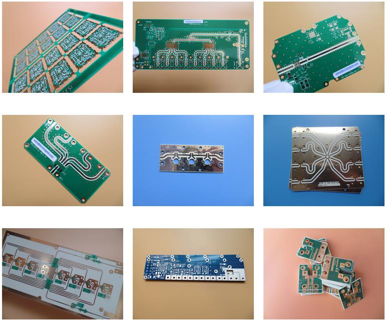
Variety of PCBs

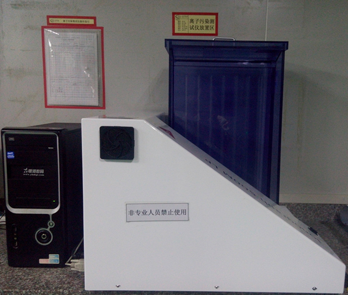
Ionic contamination tester

Just as its name implies, high frequency is that the frequency is relatively high, generally
Refers to the frequency of >=300 MHz (i.e. Wave length <=1m), that is, the usual radio
Frequency band. the electromagnetic wave of frequency >=1GHz is named microwave.
Typical frequencies for wireless applications:
* Current: 0.9GHz - 2GHz
* 3G systems: 2.5GHz
* Bluetooth: 2.5GHz
* GPS: 12.6GHz
* LMDS: 24GHz and 40GHz
* Automotive: 77GHz
Market: RFID, Wireless communications, base station and antenna, amplifier, military products,
Consumer electronics.
High frequency printed circuit board or microwave PCB refers to the printed circuit board made
on the high frequency (microwave) substrate copper clad plate. the common types are: Double
-sided board, multilayer board and mixed structure.
Mixed structure includes high performance special substrate, PP sheet + ordinary performance
Board and PP sheet mixed pressing board; high frequency substrate + ordinary FR4 substrate;
High frequency substrate + metal base etc.
PCB Case: Teflon PCB Boards Built On 20mil RO4350B
with Immersion Gold
(Printed circuit boards are custom-made products, the picture and parameters shown are
Just for reference)
General description
this is a type of double sided high frequency PCB built on RO4350B 20 mil substrate for
the application of antenna. It's a 2 layer RF PCB board at 0.6 mm thick. It's immersion
Gold finish without solder mask. It's fabricated per IPC 6012 Class 2 using supplied Gerber
Data. Each 20 boards are packed for shipment.
Features and benefits
the dielectric constant (DK) is low and stable, so the signal transmission is good without
Delay.
Excellent high frequency performance due to low dielectric tolerance and loss.
RO4003C exhibit a stable dielectric constant over a broad frequency range. this makes it
An ideal substrate for broadband applications.
SMT process is resistant to reflow soldering, resistant to rework due to gold pads.
Make delivery on time keeping 98% on-time-delivery rate.
Meeting your printed circuit board needs from PCB prototyping to mass volume production.
Fast and flexible to save the time of production from prototype to standard production
High quality helps customers win cost-saving.
UL recognized and RoHS Directive-compliant
Application
Amplifier, Transmitter combiner, Optoelectronic Transmitters, Trunk amplifier
Parameter and data sheet
| PCB SIZE | 67 x 67mm=1up |
| BOARD TYPE | Double sided PCB |
| Number of Layers | 2 layers |
| Surface Mount Components | YES |
| through Hole Components | NO |
| LAYER STACKUP | Copper ------- 35um(1 oz)+plate TOP layer |
| RO4350B 0.508mm | |
| Copper ------- 35um(1oz) + plate BOT Layer | |
| TECHNOLOGY | |
| Minimum Trace and Space: | 7.9 mil / 5.9 mil |
| Minimum / Maximum Holes: | 0.4 mm / 0.4 mm |
| Number of Different Holes: | 1 |
| Number of Drill Holes: | 3 |
| Number of Milled Slots: | 0 |
| Number of Internal Cutouts: | 0 |
| Impedance Control: | no |
| Number of Gold finger: | 0 |
| BOARD MATERIAL | |
| Glass Epoxy: | RO4350B Tg280, er<3.48, Rogers Corp. |
| Final foil external: | 1.5 oz |
| Final foil internal: | N/A |
| Final height of PCB: | 0.6 mm 0.1 |
| PLATING and COATING | |
| Surface Finish | Immersion gold, 87% |
| Solder Mask Apply to: | N/A |
| Solder Mask Color: | N/A |
| Solder Mask Type: | N/A |
| CONTOUR/CUTTING | Routing |
| MARKING | |
| Side of Component Legend | N/A |
| Colour of Component Legend | N/A |
| Manufacturer Name or Logo: | N/A |
| VIA | Plated through hole(PTH), minimum size 0.4mm. |
| FLAMIBILITY RATING | UL 94-V0 Approval MIN. |
| DIMENSION TOLERANCE | |
| Outline dimension: | 0.0059" |
| Board plating: | 0.0029" |
| Drill tolerance: | 0.002" |
| TEST | 100% Electrical Test prior shipment |
| TYPE of ARTWORK to BE SUPPLIED | Email file, Gerber RS-274-X, PCBDOC etc |
| SERVICE AREA | Worldwide, Globally. |
Variety of PCBs
Ionic contamination tester


